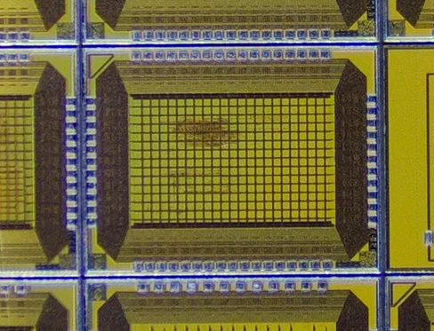
 Die shot of my Expresso chip featuring the 4-port 100Mbps Ethernet switch and the 100Mbps network connected broadcasting beacon.
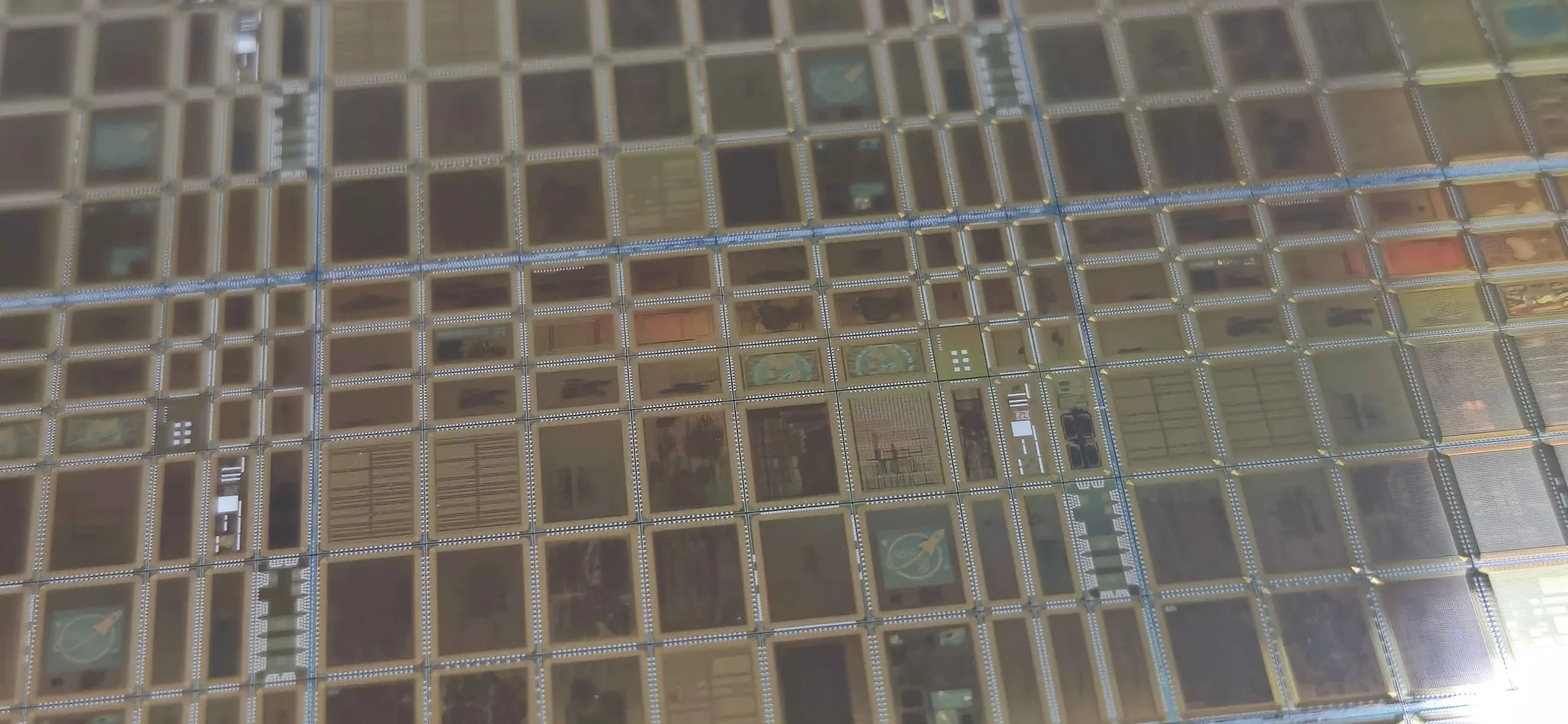 wafer.space second shuttle diced wafer, my chip is one of the small ones on the top right.
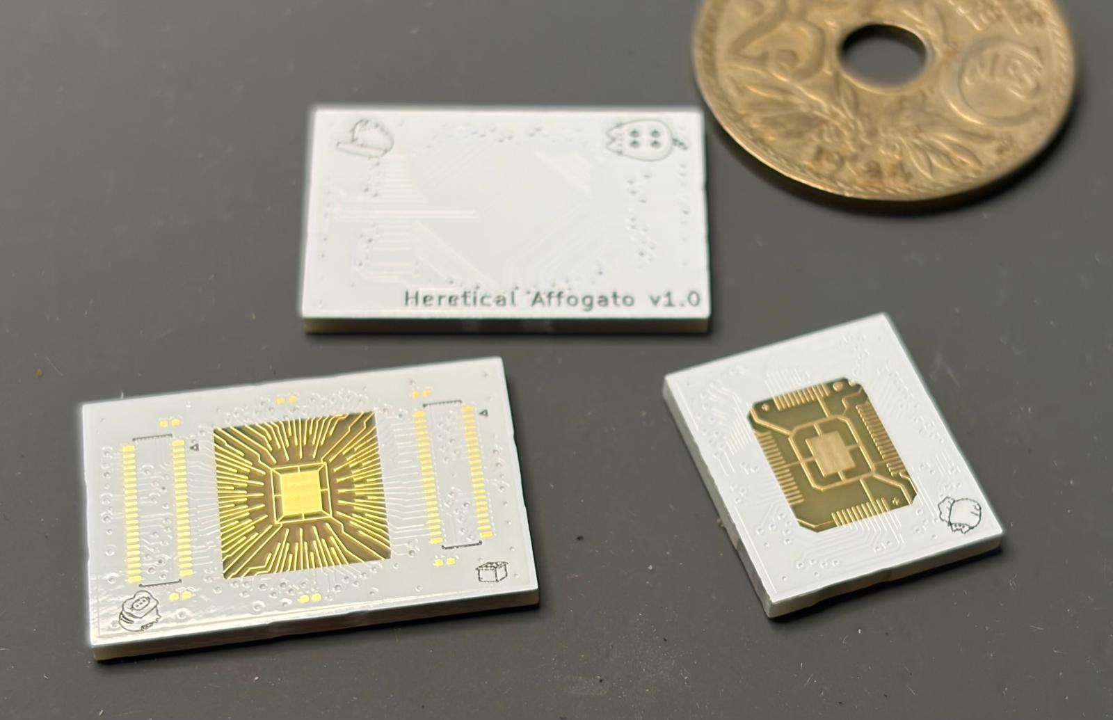 Chip-on-Board test PCBs for 56 and 76 pin parts with coin for scale.
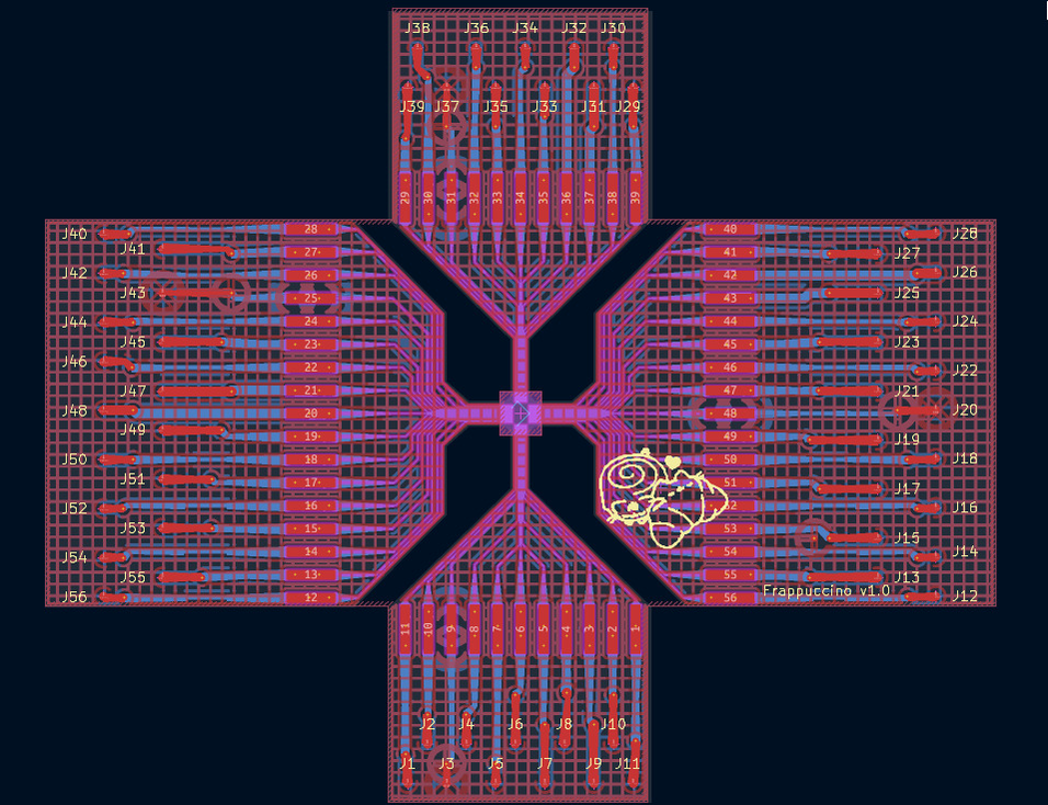 Flex PCB for an “Taped-Automatic Assembly” like ASIC packaging. Targetting the 56 pin ASIC switch chip.
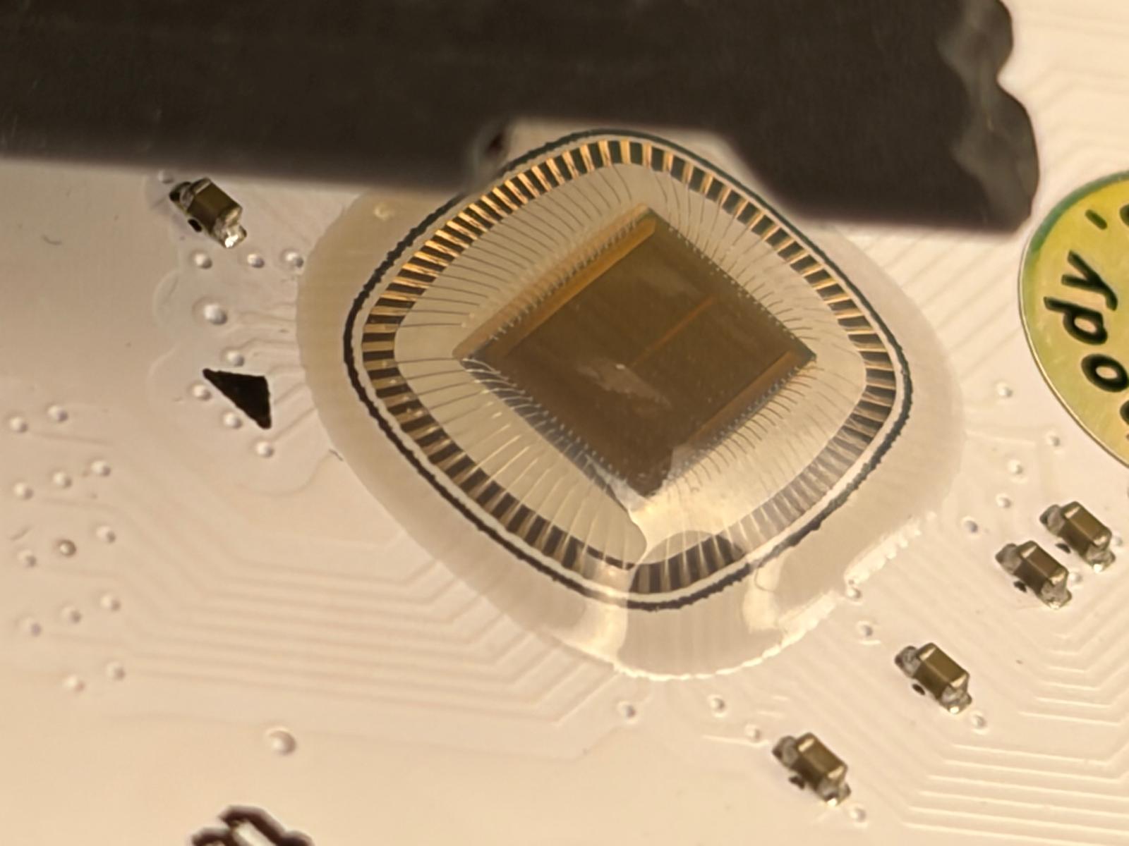 ASIC chip containing the first generation systolic array.
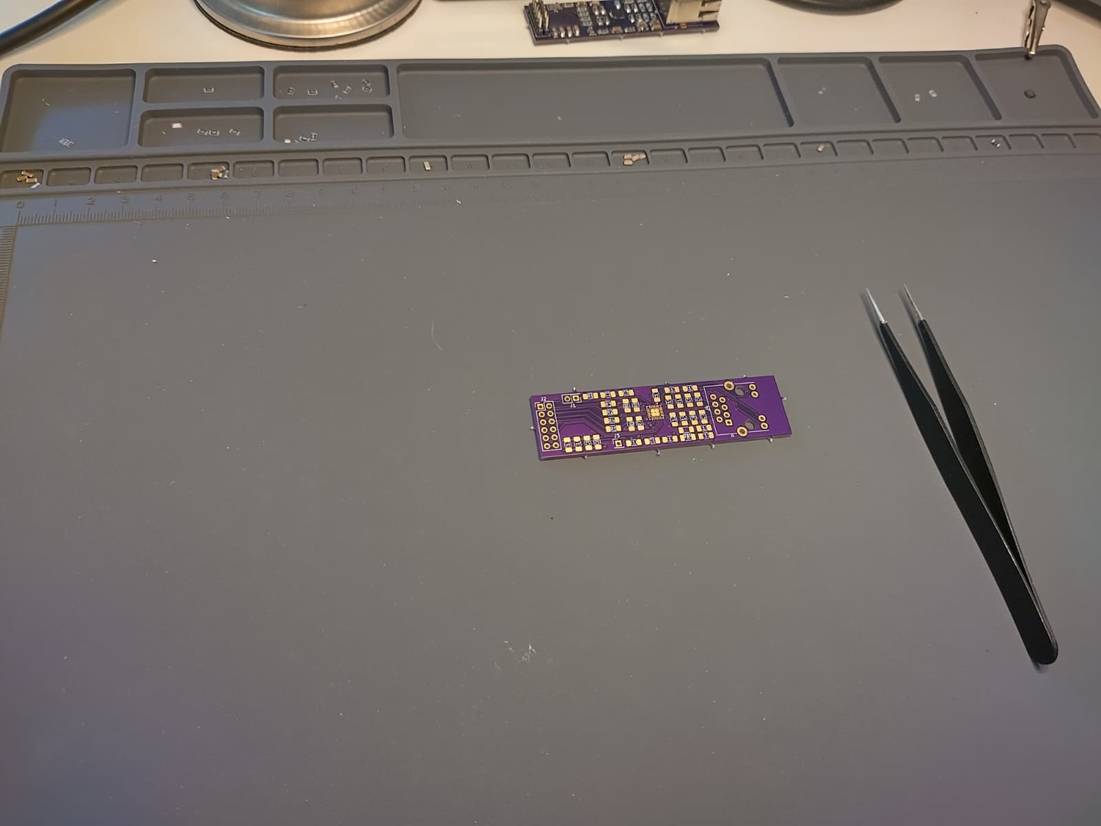 Single Ethernet connector Pmod test PCB, assembly in process.
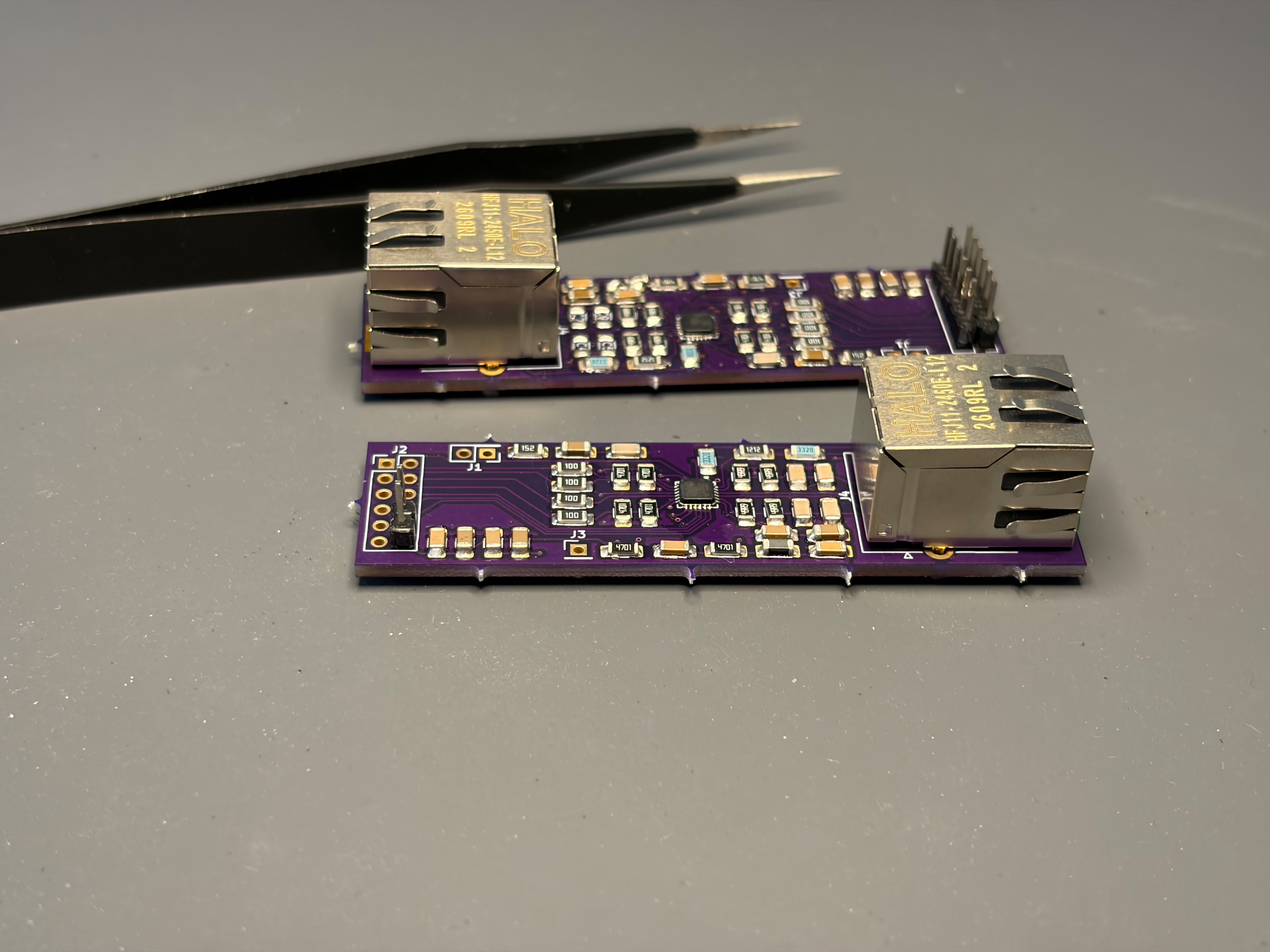 Single Ethernet connector Pmod test PCB mounted.
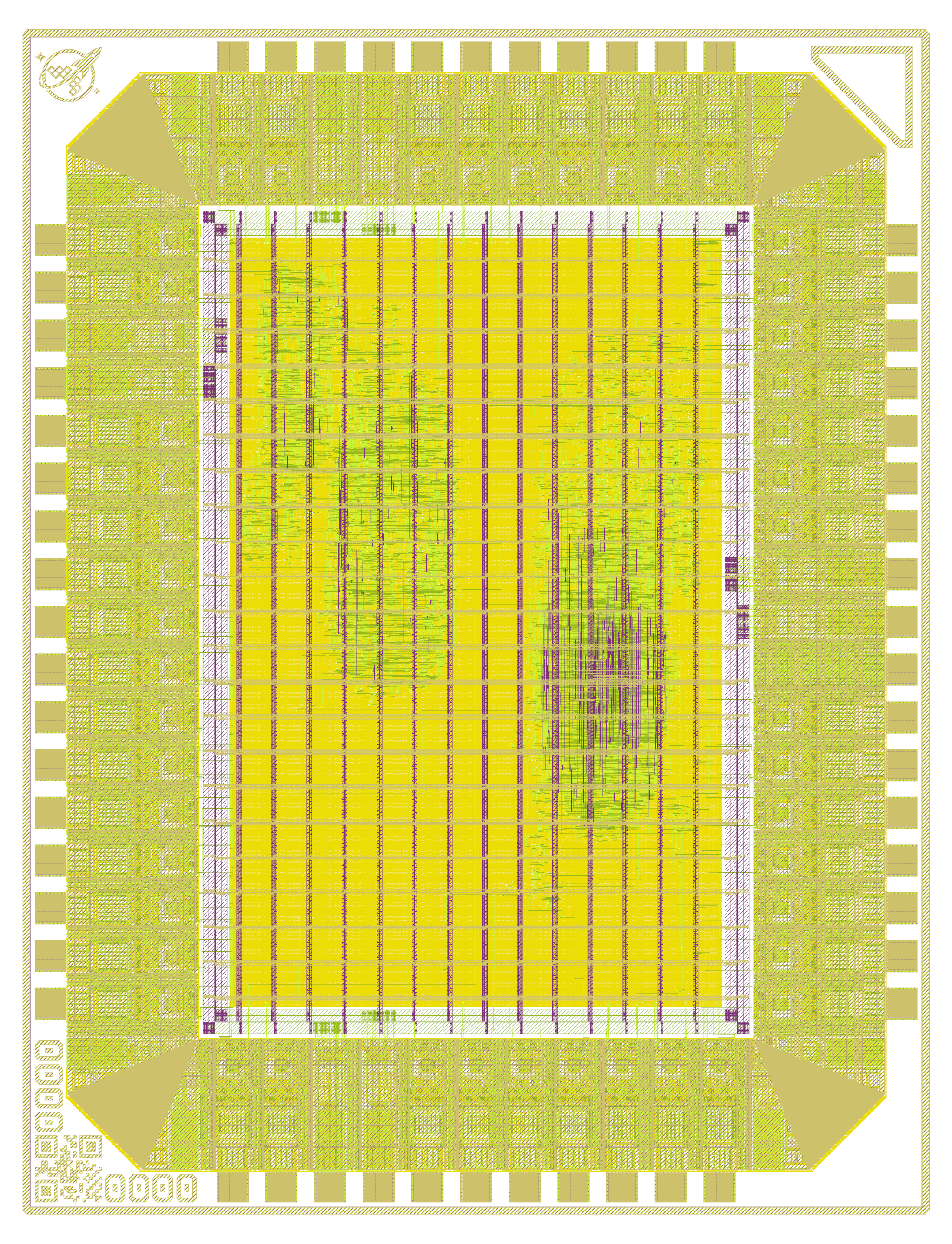 Full ASIC chip featuring a 4-port 100Mbps Ethernet switch and a beacon broadcasting over the local network. Tape-out number 10, targetting the gf180mcuD node, 1.94mm×2.53mm die area, 56 pins.
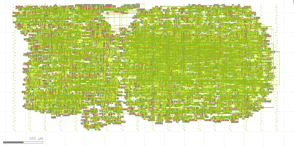 Ethernet Beacon broadcasting over 100Mbps Ethernet. Tapeout-number 9, targetting the gf180 node .
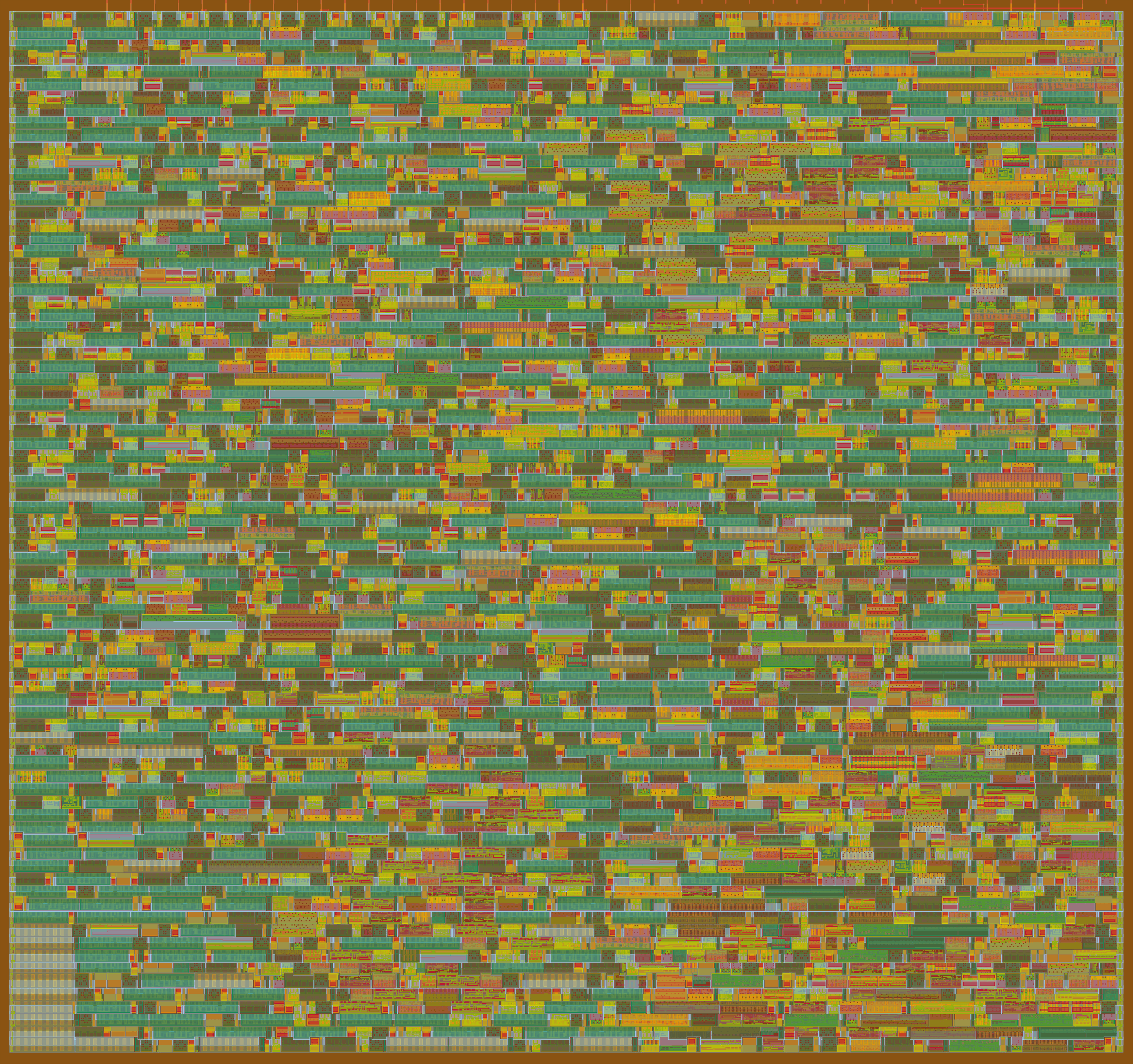 Accelerator wrapper for interfacing over 100Mbps Ethernet. Tape-out number 6, targetting the gf180mcuD node.
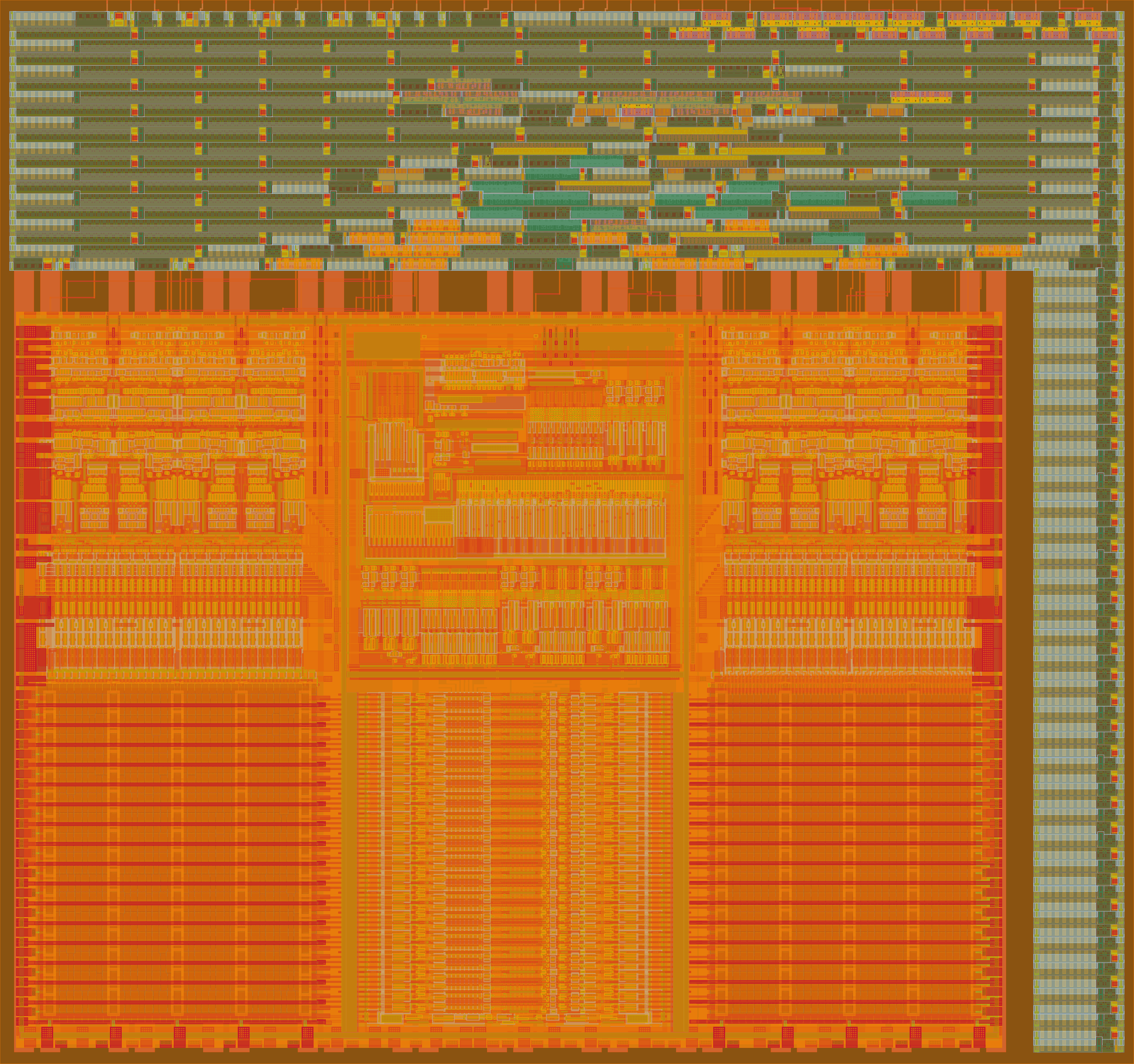 Test design for the OCD 256x8 SRAM macro. Tape-out number 8, targetting the gf180.
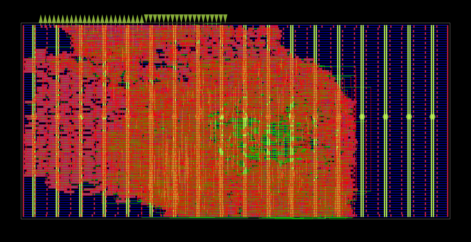 3-port 100Mbps Ethernet Switch. Tape-out number 7, targetting the gf180mcuD node.
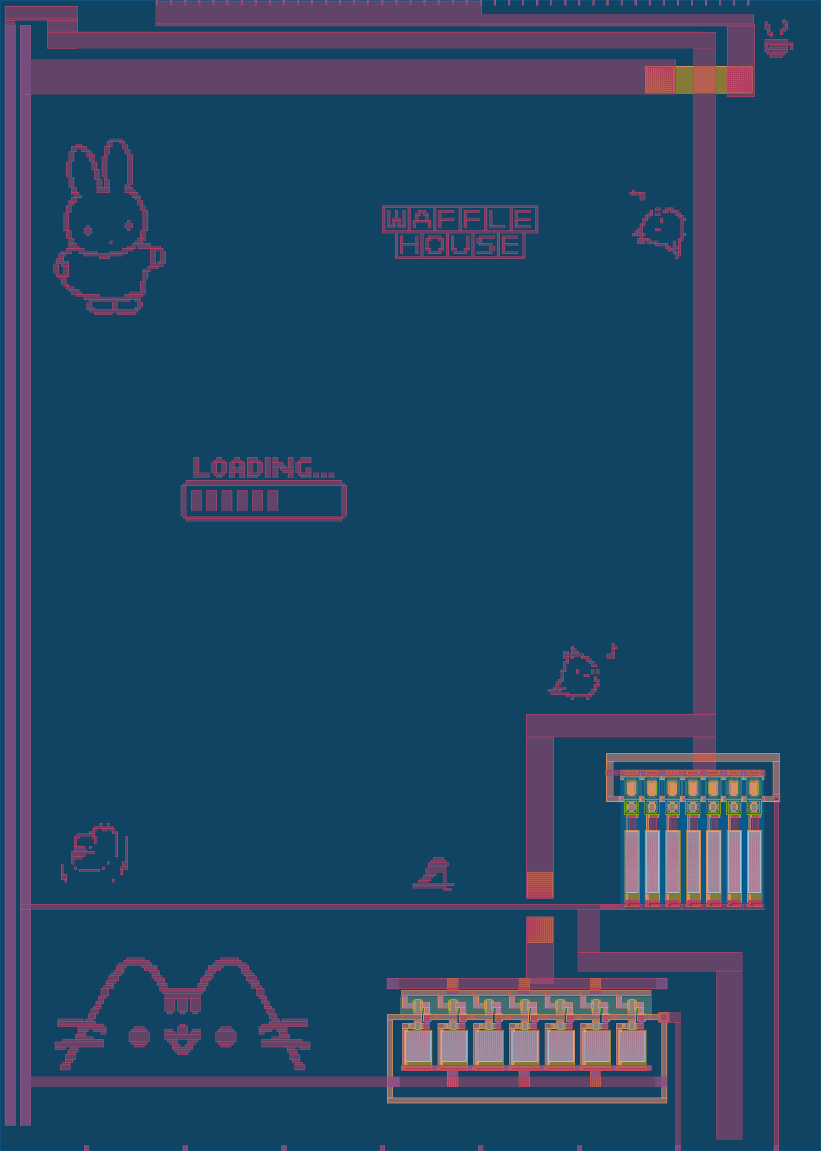 Analog 33Mhz oscillator. Tape-out number 5, targetting the sky130A node.
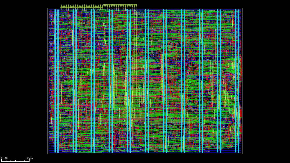 Second generation systolic array, using custom designed bfloat16 floating point math with full DFT infrastrucutre including scan-chains accessible over JTAG. Tape-out number 3, targetting the ihp130g2 node.
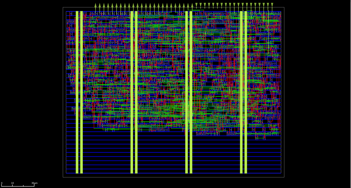 Frequency optimized custom bfloat16 multiplier. Tape-out number 4, targetting the ihp130cmos5l node.
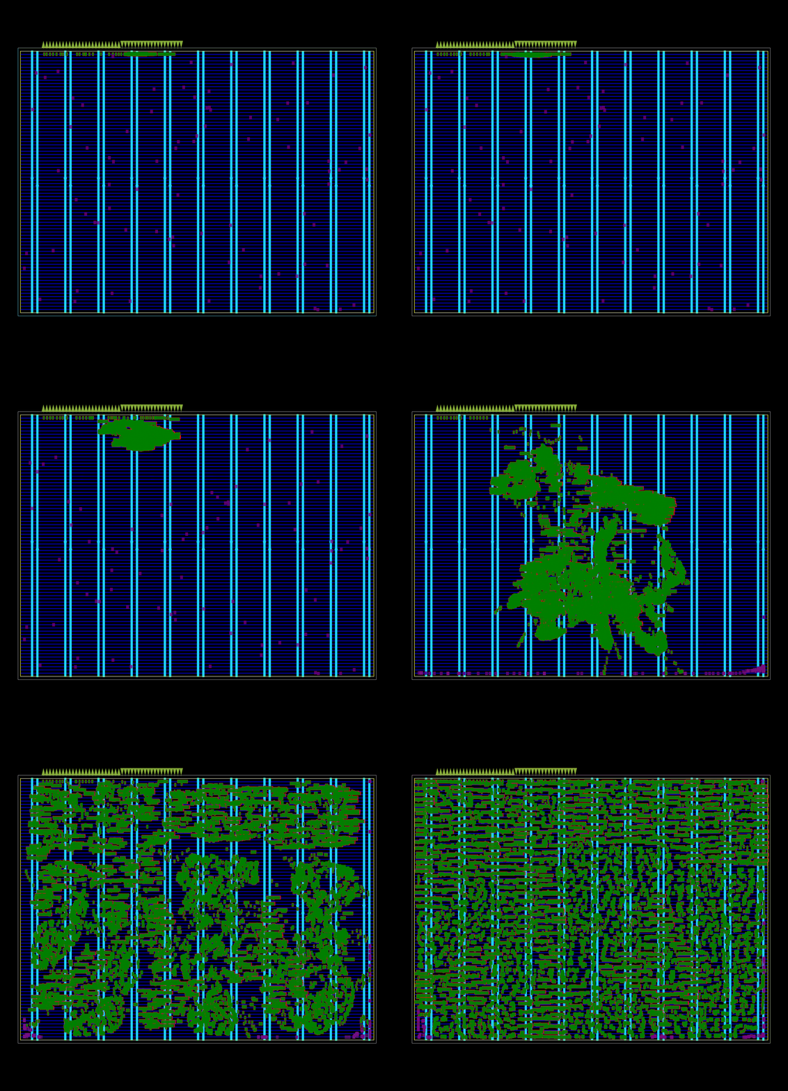 Initial global placement of the second generation systolic array. Tape-out number 3, targetting the ihp130g2 node.
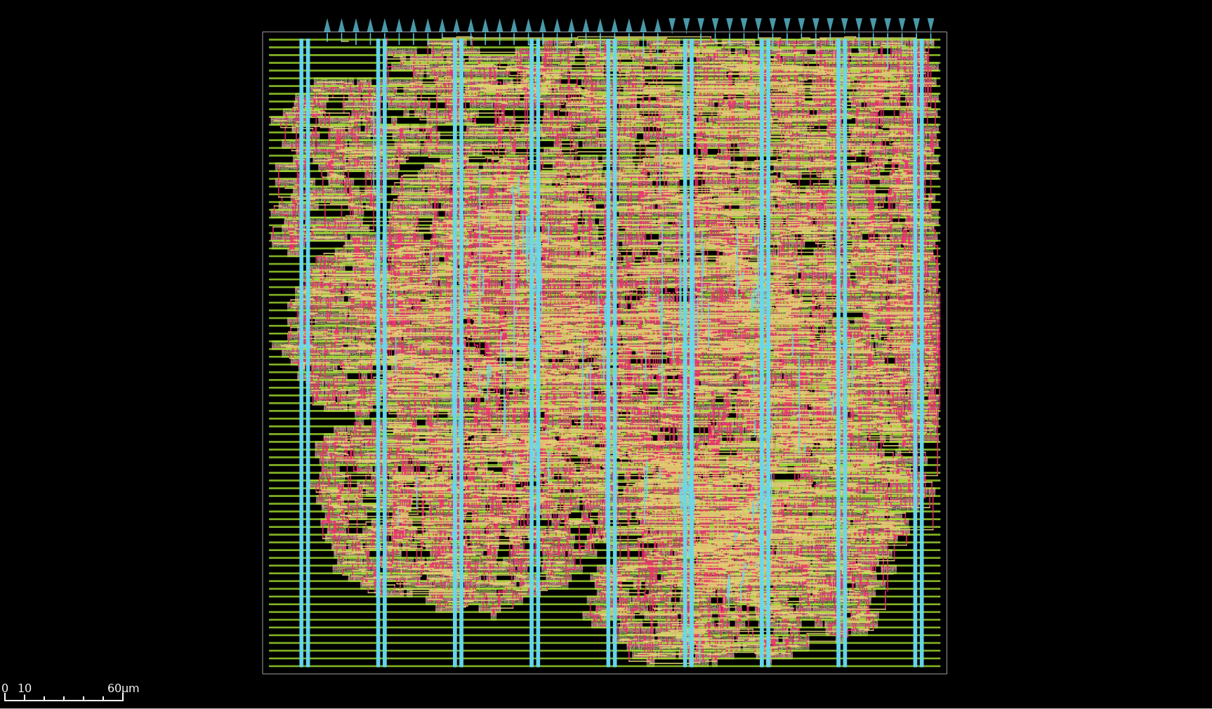 Silicon Proven at A0. First generation systolic array, using signed integers with in silicon debug infrastrucutre accessible over JTAG. Tape-out number 2, targetting the gf180mcuD node.
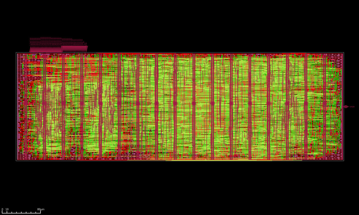 BLAKE2s hashing accelerator. Tape-out number 1, targetting the sky130A node .
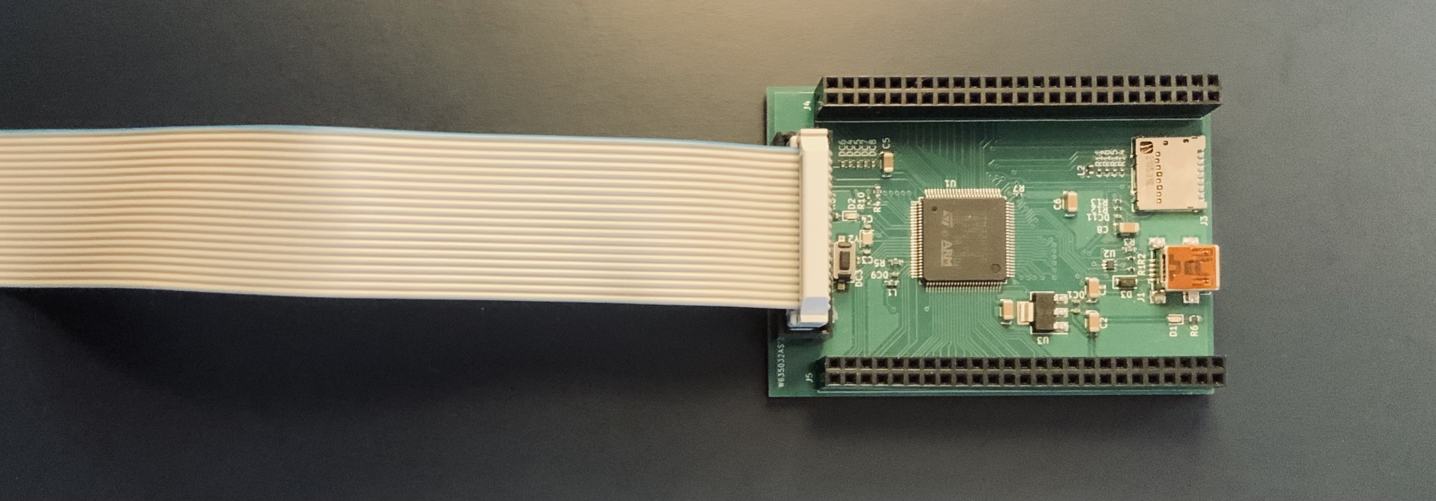 Custom STM32H7 development board designed as a 10 year anniversary present.